Hydrogels, with their bio-like mechanical properties, high water retention, and ion permeability, are extensively used in tissue engineering, medical dressings, and biosensing. Although they can become electronically conductive when combined with conductive materials, hydrogel-based electronics fall short of silicon-based devices in achieving integrated circuit functionalities like switching and amplification. Traditional organic semiconducting materials are difficult todissolveand process in aqueous solutions and cannot be combined with traditional hydrogels, nor can they achieve excellent semiconductor performance in aqueous solutions.
To address these challenges, theTing Lei Research Group at Peking University developed a strategy for creating semiconducting hydrogels, bridging the performance gap of traditional hydrogels in electronic circuits. By crosslinking water-soluble cationic conjugated polymers with counterions or blending them with other hydrogels to form multi-network structures, they produced semiconducting hydrogels with superior mechanical, semiconducting, and bio-interface properties (Figure 1). For the first time, they realized semiconducting hydrogel devices and logic circuits with excellent switching characteristics based on semiconducting hydrogels and achieved high signal-to-noise ratio amplification of bioelectric signals in situ. This work was published in Science as“N-type Semiconducting Hydrogel”.
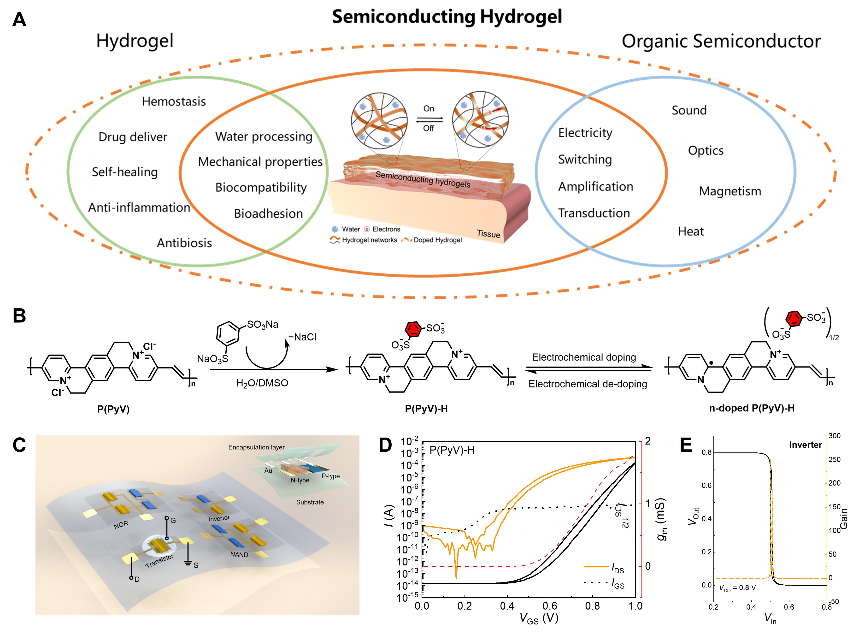
Figure 1. Structure, doping mechanisms, and device performance of semiconducting hydrogels: A) Semiconducting hydrogels possess a variety of characteristics of both traditional hydrogels and organic semiconductors; B) Counterion crosslinking mechanism and electrochemical doping mechanism of the polymer P(PyV); C-E) Complementary logic circuits constructed from semiconducting hydrogels and their performance.
The conjugated polymer, P(PyV), can also be combined with various traditional hydrogels to construct multi-network hydrogel materials (Figure 2A). The multi-network semiconducting hydrogels exhibit good mechanical stretchability and bioadhesion. They also demonstrate semiconducting performance comparable to single-network hydrogels and can achieve various circuit functions such as switching, logic gates, and signal amplification.
These semiconducting hydrogels have good biocompatibility, allowing them to be directly used as the interface between bioelectronic devices and tissues. The inverter made from semiconducting hydrogels exhibitsa better amplification gain than traditional organic semiconductor logic devices, capable of amplifying small signals. For an input of AC small signals in the range of 1-100 Hz, the maximum gain can reach 79 V/V. Based on the complementary semiconducting hydrogel signal amplifier, the authors have achieved high signal-to-noise ratio amplification of various electrophysiological signals (Figures 2B-D).
This research pioneers the fabrication and electronic application of high-performance semiconducting hydrogels.These semiconductinghydrogels combine the excellent electrical properties of organic semiconductors with the unique mechanical and biointer face characteristics of hydrogels, expanding the application range of both organic semiconductors and hydrogel materials.The semiconducting hydrogels facilitate the development of diverse logic circuits, and their amplifiers notably boost the signal-to-noise ratio of faint biosignals, offering an innovative method for effective biosignal capture.
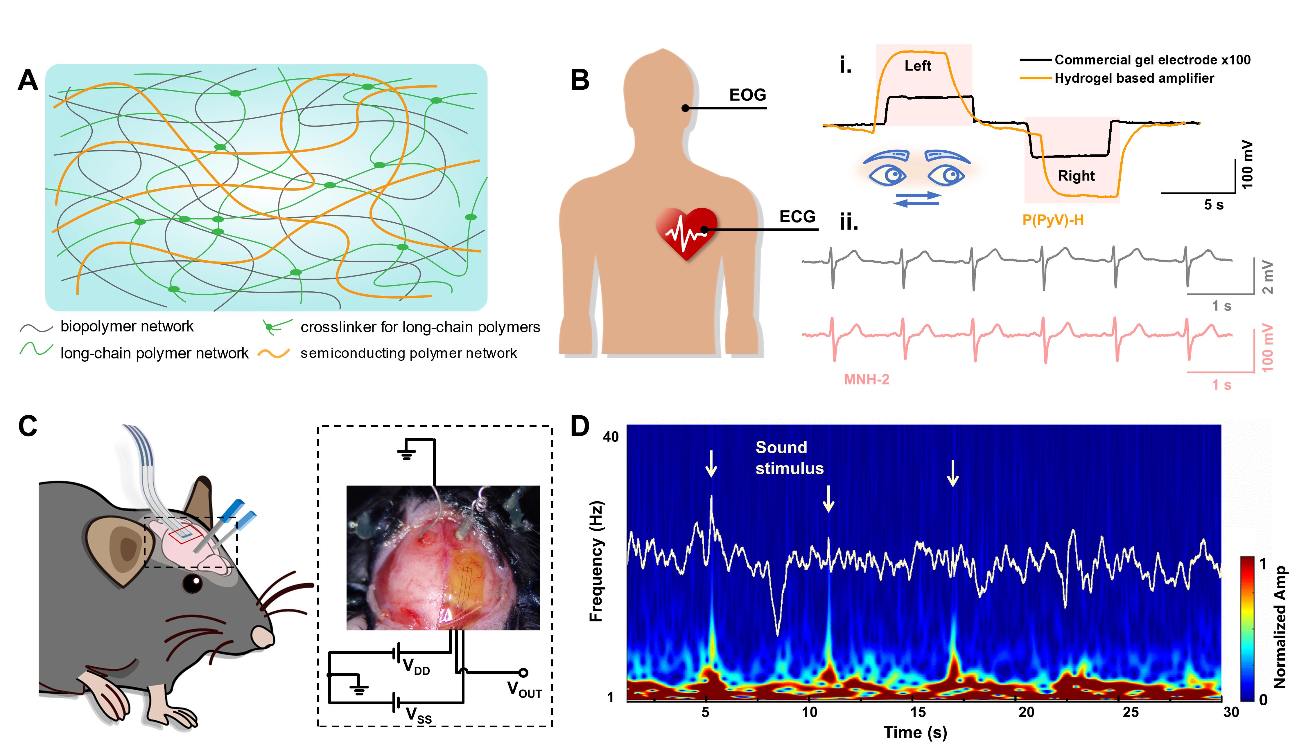
Figure 2. Bioelectronic applications based on semiconducting hydrogels: A) Schematic diagram of the multi-network hydrogel; B) Schematic diagram and signal amplification performance of ECG and EOG tests; C-D) Schematic diagram and results of in vivo EEG signal acquisition from a mouse.
Doctoral students Peiyun Li and Wenxi Sun are the co-first authors of the paper, and Prof.T ingLei is the corresponding author. Collaborators include the Xiaochuan Dairesearch group from Tsinghua University, the Shixian Lv research group from Peking University, and the Jia Zhu research group from the National Center for Nanoscience and Technology. This research was supported by the National Natural Science Foundation of China, the Beijing Natural Science Foundation, the High-Performance Computing Platform of Peking University, the Materials Processing and Testing Center of Peking University, the Molecular Materials and Nanofabrication Laboratory (MMNL) at the College of Chemistry and Molecular Engineering of Peking University, and the Shanghai Synchrotron Radiation Facility.